Poland Gallium Nitride (GaN) Substrate Market Size and Insights – 2026 to 2033
Report ID : IL_17418 | Report Language's : En/Jp/Fr/De | Publisher : IL |
Format : 


What is the Market Size of the Poland Gallium Nitride (GaN) Substrate in 2026?
The Poland Gallium Nitride (GaN) Substrate Market Size in 2026 is estimated to be $125.0 Million USD
What is the Growth Rate (CAGR) of Poland Gallium Nitride (GaN) Substrate Market?
The Poland Gallium Nitride (GaN) Substrate Market is expected to grow at 25.5% CAGR
What is the Market Size of the Poland Gallium Nitride (GaN) Substrate in 2033?
The Poland Gallium Nitride (GaN) Substrate Market Size in 2033 is estimated to be $565.0 Million USD

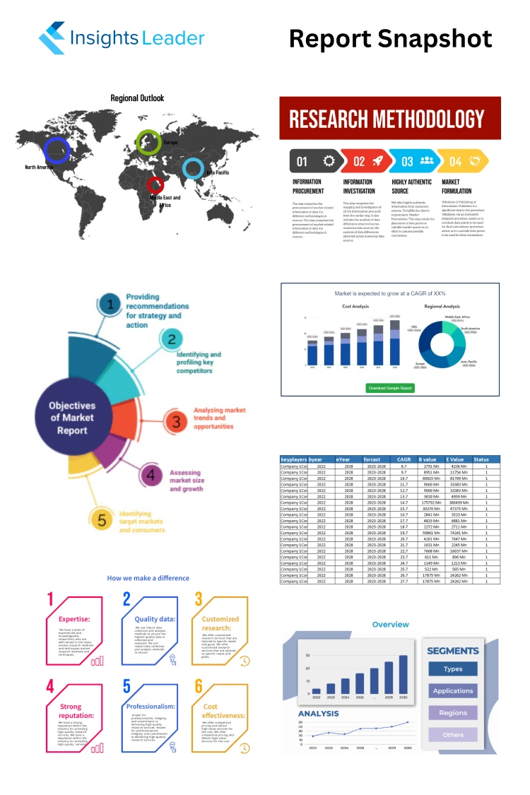
Report Snapshot
| Report Attributes | Report Details |
|---|---|
| Forecast Year | 2033 |
| CAGR | 25.5% |
| History Year | 2016-2024 |
| Market Size in 2026 | 125.0 Million USD |
| Market Size in 2033 | 565.0 Million USD |
What are DRO and Impact Forces of Poland Gallium Nitride (GaN) Substrate Market?
Drivers include accelerated adoption of 5G infrastructure, increasing demand for high-efficiency power electronics in Electric Vehicles (EVs), and governmental emphasis on energy conservation mandates. Restraints primarily involve the high production cost of native GaN substrates and manufacturing complexities related to crystal defect density. Opportunities reside in defense, aerospace, and high-frequency radar systems.
What is Impact of U.S. Tariffs on Poland Gallium Nitride (GaN) Substrate Market?
The impact of U.S. tariffs on the Polish GaN substrate market is largely indirect, affecting the global semiconductor supply chain and component pricing. While Poland itself may not be a primary target of specific tariffs, global trade tensions increase raw material costs and can disrupt the sourcing of specialized equipment necessary for GaN processing. This ultimately influences the final product cost and market accessibility within the EU framework.
How is AI currently impacting Poland Gallium Nitride (GaN) Substrate Market?
AI is primarily utilized to optimize the epitaxy process, enhancing crystal growth simulation models to minimize defects and maximize wafer yield, thereby addressing a core manufacturing challenge. Furthermore, AI-driven automated inspection and quality control systems are deployed in advanced facilities, ensuring higher uniformity and reliability for mission-critical applications like high-power data centers and telecommunications amplifiers.
Poland Gallium Nitride (GaN) Substrate Market Research Report – Table of Contents
1. Executive Summary
2. Introduction & Research Objectives
3. Scope of the Study
4. Research Methodology of Poland Gallium Nitride (GaN) Substrate Market
5. Poland Gallium Nitride (GaN) Substrate Market Overview & Industry Background
6. Poland Gallium Nitride (GaN) Substrate Market Size & Forecast Analysis
7. Poland Gallium Nitride (GaN) Substrate Market Segmentation Analysis
8. Competitive Landscape
9. Consumer Behavior & Demand Analysis
10. Pricing & Cost Structure Analysis
11. Poland Gallium Nitride (GaN) Substrate Market Drivers, Challenges & Risks
12. Regulatory & Policy Framework
13. Technology & Innovation Impact
14. Strategic Insights & Recommendations
15. Conclusion & Future Outlook
For more queries, kindly contact [email protected]