Asia-Pacific Gallium Nitride (GaN) Substrate Market Size and Insights – 2026 to 2033
Report ID : IL_18178 | Report Language's : En/Jp/Fr/De | Publisher : IL |
Format : 


What is the Market Size of the Asia-Pacific Gallium Nitride (GaN) Substrate in 2026?
The Asia-Pacific Gallium Nitride (GaN) Substrate Market Size in 2026 is estimated to be XXX Mn
What is the Growth Rate (CAGR) of Asia-Pacific Gallium Nitride (GaN) Substrate Market?
The Asia-Pacific Gallium Nitride (GaN) Substrate Market is expected to grow at XX%
What is the Market Size of the Asia-Pacific Gallium Nitride (GaN) Substrate in 2033?
The Asia-Pacific Gallium Nitride (GaN) Substrate Market Size in 2033 is estimated to be XXX Mn

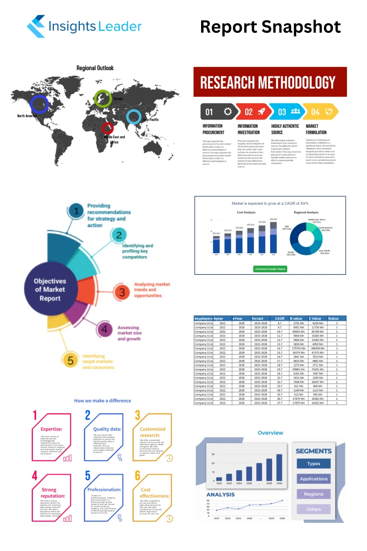
Report Snapshot
| Report Attributes | Report Details |
|---|---|
| Forecast Year | 2033 |
| CAGR | XX% |
| History Year | 2016-2024 |
| Market Size in 2026 | XXX Mn |
| Market Size in 2033 | XXX Mn |
What are DRO and Impact Forces of Asia-Pacific Gallium Nitride (GaN) Substrate Market?
The primary drivers include the massive deployment of 5G telecommunication networks and the increasing integration of GaN in power electronics for electric vehicles (EVs) and consumer fast chargers. Restraints center on the high production cost of native GaN wafers and competition from Silicon Carbide (SiC) in high-power applications. Opportunities exist in defense radar systems and advanced microLED displays, pushing demand for high-quality substrates.
What is Impact of U.S. Tariffs on Asia-Pacific Gallium Nitride (GaN) Substrate Market?
U.S. tariffs and subsequent trade restrictions primarily affect the geopolitical certainty surrounding the supply chain of GaN-based devices and specialized manufacturing equipment. This environment accelerates regional initiatives, particularly in China and South Korea, to achieve full self-sufficiency in native GaN substrate production. This mitigation strategy minimizes reliance on external sources for critical semiconductor materials.
How is AI currently impacting Asia-Pacific Gallium Nitride (GaN) Substrate Market?
AI is revolutionizing the epitaxial growth phase by deploying machine learning algorithms to monitor and optimize crystal growth parameters in real-time, resulting in superior material uniformity and significantly reduced defect densities. Furthermore, the massive power demand from AI data centers drives indirect demand for highly efficient GaN power devices, stimulating innovation and capacity expansion within the substrate manufacturing sector.
Asia-Pacific Gallium Nitride (GaN) Substrate Market Research Report – Table of Contents
1. Executive Summary
2. Introduction & Research Objectives
3. Scope of the Study
4. Research Methodology of Asia-Pacific Gallium Nitride (GaN) Substrate Market
5. Asia-Pacific Gallium Nitride (GaN) Substrate Market Overview & Industry Background
6. Asia-Pacific Gallium Nitride (GaN) Substrate Market Size & Forecast Analysis
7. Asia-Pacific Gallium Nitride (GaN) Substrate Market Segmentation Analysis
8. Competitive Landscape
9. Consumer Behavior & Demand Analysis
10. Pricing & Cost Structure Analysis
11. Asia-Pacific Gallium Nitride (GaN) Substrate Market Drivers, Challenges & Risks
12. Regulatory & Policy Framework
13. Technology & Innovation Impact
14. Strategic Insights & Recommendations
15. Conclusion & Future Outlook
For more queries, kindly contact [email protected]