Belgium Gallium Nitride (GaN) Substrate Market Size and Insights – 2026 to 2033
Report ID : IL_18098 | Report Language's : En/Jp/Fr/De | Publisher : IL |
Format : 


What is the Market Size of the Belgium Gallium Nitride (GaN) Substrate in 2026?
The Belgium Gallium Nitride (GaN) Substrate Market Size in 2026 is estimated to be USD 45.0 Million
What is the Growth Rate (CAGR) of Belgium Gallium Nitride (GaN) Substrate Market?
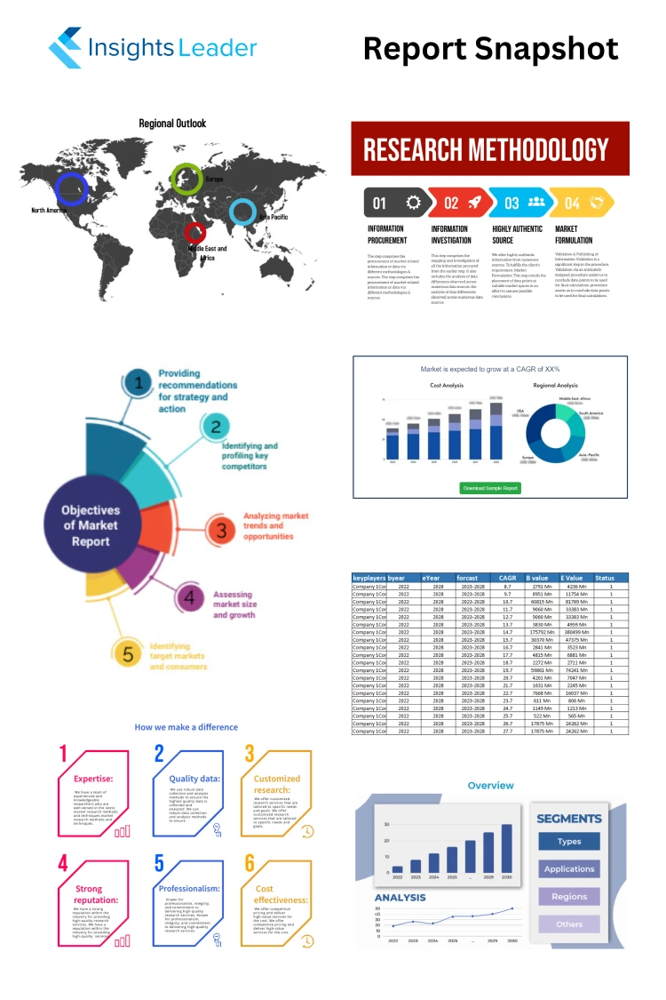
The Belgium Gallium Nitride (GaN) Substrate Market is expected to grow at CAGR 28.5%
What is the Market Size of the Belgium Gallium Nitride (GaN) Substrate in 2033?
The Belgium Gallium Nitride (GaN) Substrate Market Size in 2033 is estimated to be USD 260.0 Million

Report Snapshot
| Report Attributes | Report Details |
|---|---|
| Forecast Year | 2033 |
| CAGR | 28.5% |
| History Year | 2016-2024 |
| Market Size in 2026 | 45.0 Million USD |
| Market Size in 2033 | 260.0 Million USD |
What are DRO and Impact Forces of Belgium Gallium Nitride (GaN) Substrate Market?
Drivers include rapid deployment in 5G telecommunication infrastructure and the increasing demand for high-efficiency power electronics in Electric Vehicles (EVs) across Europe. Restraints primarily involve the high production cost of native GaN substrates and technological challenges associated with large-area substrate fabrication. Opportunities arise from expanding military radar and aerospace satellite communication applications.
What is Impact of U.S. Tariffs on Belgium Gallium Nitride (GaN) Substrate Market?
U.S. tariffs primarily induce supply chain volatility, affecting the import pricing of essential manufacturing equipment and precursor materials sourced globally. This external pressure can elevate the operational expenditure for GaN fabricators in Belgium, potentially slowing investment in domestic expansion and R&D for next-generation devices.
How is AI currently impacting Belgium Gallium Nitride (GaN) Substrate Market?
AI significantly enhances material quality by optimizing MOCVD growth parameters using machine learning to minimize crystal defects and maximize yield. Furthermore, AI-driven Electronic Design Automation (EDA) tools accelerate the simulation and validation of GaN power and RF device layouts, critically reducing the design cycle time for complex semiconductor components.
Belgium Gallium Nitride (GaN) Substrate Market Research Report – Table of Contents
1. Executive Summary
2. Introduction & Research Objectives
3. Scope of the Study
4. Research Methodology of Belgium Gallium Nitride (GaN) Substrate Market
5. Belgium Gallium Nitride (GaN) Substrate Market Overview & Industry Background
6. Belgium Gallium Nitride (GaN) Substrate Market Size & Forecast Analysis
7. Belgium Gallium Nitride (GaN) Substrate Market Segmentation Analysis
8. Competitive Landscape
9. Consumer Behavior & Demand Analysis
10. Pricing & Cost Structure Analysis
11. Belgium Gallium Nitride (GaN) Substrate Market Drivers, Challenges & Risks
12. Regulatory & Policy Framework
13. Technology & Innovation Impact
14. Strategic Insights & Recommendations
15. Conclusion & Future Outlook
For more queries, kindly contact [email protected]